NE555 is an IC which is used widely in electronics. It can be used in 3 modes which are called: ASTABLE, MONOSTABLE and BISTABLE. The 555 can be used in pulse generation, timing process and as an ossilator. We will use it in ASTABLE mode in order to generate continuous square wave.
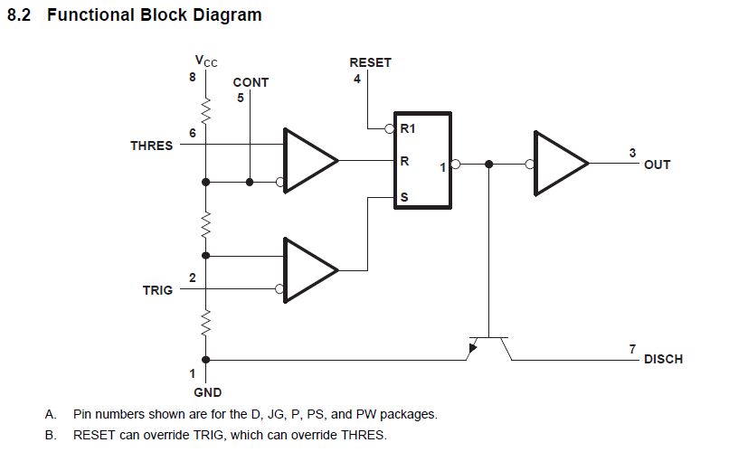
The 555 IC consists of three resistors, two comparators, one flip-flop, one not gate and one NPN transistor. These three resistors have 5KΩ resistance values, and they serve as voltage divider. The 555 takes its name from these resistors.
The first node has 2/3 of Vcc voltage value and the second one has 1/3 of Vcc voltage value (if you dont know what the voltage divider is, you can learn it easily from my Voltage Dividers content(in Turkish)).
Using the application, we can easily understand how this timer works. If we apply more then 2/3 of Vcc for a threshold pin, the first comparator’s output will be 1 and this output is connected to reset terminal of flip-flop and then flip-flop’s output will be 0. Otherwise if we apply less than 1/3 of Vcc voltage for trigger pin second comparator’s output, which is connected to set terminal of flip-flop, will be 1.
The discharge pin is connected to the ground via NPN transistor. Thanks to this pin we will discharge our capacitor.
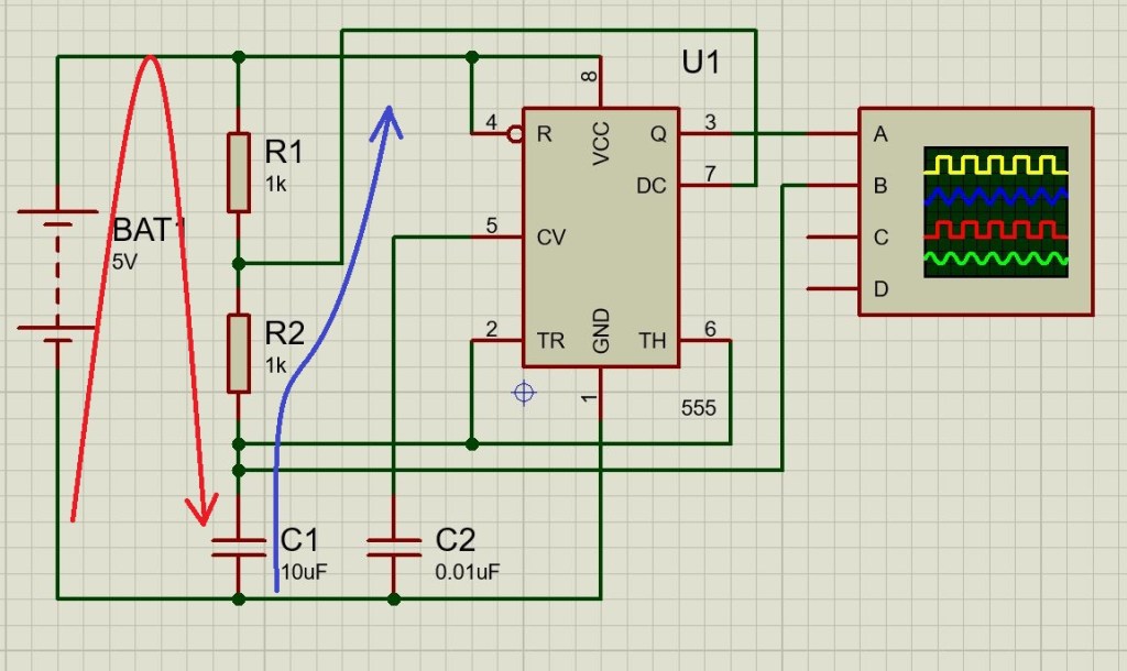
When you look at this circuit first it can seem to be difficult to understand but we are just using basic RC fundamentals. Let’s examine the circuit step by step!
C1 capacitor is charging on the red path by using R1 and R2 resistors. When it achieves the 2/3 of Vcc voltage, the threshold pin triggers first comparator and this makes Flip-Flop’s out 1. Out pin becomes 0 and discharge pin starts to discharge C1 capacitor on the blue path by using R2 resistor. When charge of C1 reaches 1/3 of Vcc, trigger pin sets second comparator and Flip-Flop out. Then out pin becomes 1 and C1 starts charging again. Next this cycle is repeated. C1 capacitor will be charged and discharged between 1/3 and 2/3 of Vcc.
To achieve better signal, datasheet claims that we should put C2 capacitor on control pin, and connect reset pin to the power line.
When I started using NE555, I tried to apply RC circuit formulas to calculate parameters of this square wave. However, I could not do it because this capacitor is not charging from 0V. In RC circuit formulas charging formula does not have any initial voltage value. Therefore, in this content I will use formulas from NE555 datasheet. However, I will try to apply these RC formulas to the 555 and write a new content about it. Now let’s use the formulas which are provided by producer.
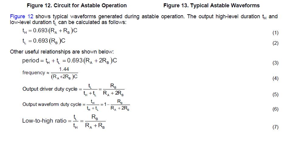
As we said before, capacitor is charging by using R1 and R2 and in this moment output stays logic 1. Therefore, by calculating charging time of C1 we can achieve the pulse width of signal. Datasheet says that time of logic 1 is equal to 0.693x(R1+R2)xC.
Whereas, for low level time we use only R2 values because capacitor is discharging on blue path by using ONLY R2 time, for low level we use 0.693x(R2)xC.
You can see other formulas in the photo.
I use 10 uF capacitor as C1 and 1 kΩ resistors. Let’s calculate frequency and duty cycle of this square wave.
Frequency = 1.44/((R1+2R2)*C)
= 1.44/((1k+2*1k)*10uF))
= 48 Hz
Duty cycle = 1-((R2/(R1+2R2)))
= 1-(1/3)
=0.666 in a sense %66.6
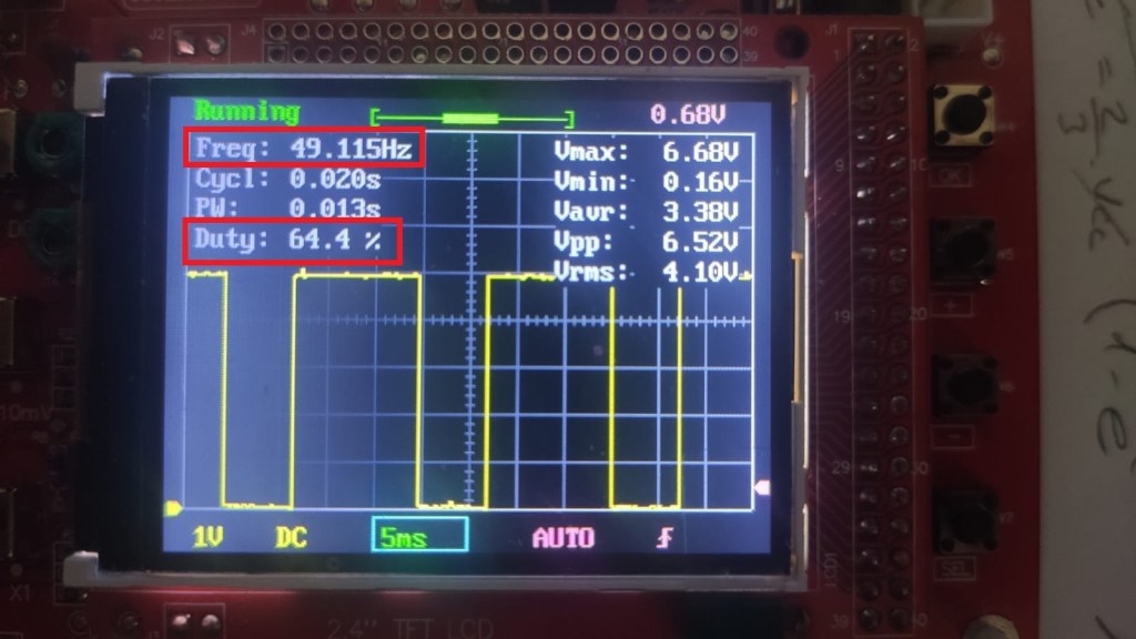
As it is visible on the ossiloscope, we do not have these parameters on practice. There are some differences between theory and practice. But why?
First things which come to my mind are tolerance values of components. When I measured these resistors my multimeters show that they have resistance values around 980Ω.
I do not have multimeter which can measure capacitors. But, as I used two different 10uF capacitors and I got different frequencies from output. Then I realised that capacitors also have tolerant values.
Lastly, when I started to work on this circuit I realised that we cannot produce a square wave which has 50% duty cycle. Because, for 50% duty cycle we have R1+R2 = R2 formula and in this formula R1 is equal to 0, but we cannot remove the R1 resistor from this circuit.
I saw some methods on the Internet in which people use R2 resistor’s value 100 times or even higher than R1 resistor. By this way you can be close to 50% duty cycle but even in theory it is not 50% duty cycle. This will be the topic of another content. 🙂
I want to say thanks to Ewa Merta for helping me with editing.
